Researchers from ATAP have demonstrated the first on-demand quantum light source in silicon, potentially laying the groundwork for a quantum internet.
A quantum internet, in which a network of interconnected quantum computers transmits, computes, and receives information encoded in quantum states, would provide new functions such as quantum cryptography and quantum cloud computing that promise unparalleled security and unimaginably high speeds and could enable new research possibilities and scientific breakthroughs.
Now, researchers from Berkeley Lab’s Accelerator Technology & Applied Physics (ATAP) Division, in collaboration with colleagues from the Lab’s Materials Science Division and Molecular Foundry and the Departments of Electrical Engineering & Computer Sciences and Materials Science & Engineering at the University of California, Berkeley, have demonstrated the first on-demand quantum light source using silicon. The technology allows single photons to be controlled and could lead to quantum networking devices that form the backbone of a quantum internet.
While there are several types of quantum light sources being explored, including entangled photons from light emitting defects and quantum dots, says Thomas Schenkel, a Senior Scientist who heads ATAP’s Fusion Science & Ion Beam Technology Program, “creating a scalable platform capable of storing, processing, and transmitting quantum information that can be integrated with existing technologies is a formidable challenge.”
To address these challenges, the researchers turned to silicon.
“Although silicon is the most scalable optoelectronic material, it is a poor light emitter,” explains Boubacar Kanté, Associate Professor of Electrical Engineering and Computer Sciences at the University of California, Berkeley, who led the research. “It turns out, however, that this is only true for classical light sources; for quantum light sources, it’s not a problem.”
Kanté notes that while single-photon light emitters in silicon have been around since the late 1980s, it has “only been in the last couple of years that individual light emitting centers have been isolated.”
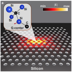
These light emitters, called color centers, are microscopic defects introduced into silicon crystals. While these centers can take several forms, G-centers—in which a pair of substitutional carbon atoms bind to the same silicon interstitial atom—have attracted considerable attention for making integrated photonic platforms with single-photon emitters.
Because G-centers emit photons in the telecommunication band, offer high spectral stability, and are bright emitters, they have “emerged as promising candidates for making quantum information platforms,” says Schenkel.
“As these centers are silicon-based, they could also be mass-produced using standard complementary metal-oxide semiconductor (CMOS) manufacturing processes employed in the semiconductor industry to make integrated circuits.”
To create the G-centers, the researchers used an ion beam to implant carbon atoms into an approximately 200-nanometer-thick layer on a silicon wafer. This implantation was followed by electron beam lithography, dry etching, thermal annealing, and wet etching, conventional processes used in the semiconductor industry.
According to Kanté, rapid thermal annealing is required to thermally cure the broad luminescence from G-centers induced by the dry etching.
“However,” he explains, “these centers emit photons at a rate that is still too slow to be useful as a quantum light source. So, to increase their emission rate, we positioned them in a photonic cavity, which forces the light emitting defect to become brighter and to emit photons at higher rates.”
He says this resulted in an eight-fold increase in their photon emission rate.
The team, he added, took a “probabilistic approach” to fabricating the centers. “This involved repeatedly carrying out the fabrication processes to increase the probability of creating centers with the desired characteristics.” The fabrication processes, he noted, were partially conducted at Berkeley Lab’s Molecular Foundry and the Marvel Nanofabrication Laboratory at the University of California, Berkeley.
The work shows for the first time that light-emitting centers the size of a few atoms can be successfully embedded in a micron-sized cavity less than one-tenth the width of a human hair. It provides a better understanding of how quantum light sources are formed in silicon and deeper insights into their properties and characteristics.
“We are now preparing a database of the different color centers predicted by theory to exist in silicon,” says Schenkel. “This will help us to identify the most suitable ones for use in selected quantum applications, including quantum computing, quantum sensing, and quantum networking devices.”
The research, he adds, is part of an ongoing collaboration between ATAP and the University of California, Berkeley, which aims to identify the best color centers for potential application in quantum information transmission and processing.
“Advances in quantum information science benefit from collaborations such as this one,” says ATAP Division Director Cameron Geddes, “where leading expertise in several critical areas, from semiconductor device fabrication to quantum optics and accelerator science and color center optimization, comes together to enable leaps in our basic understanding towards real-world applications.”
The National Science Foundation and the U.S. Department of Energy Fusion Energy Science primarily supported the research presented here. Additional funding came from the Office of Naval Research, the Moore Inventor Fellows program, and the University of California, Berkeley Bakar Fellowship.
Learn More
- Redjem, W., Zhiyenbayev, Y., Qarony, W., Ivanov, V., Papapanos, C., Liu, W., Jhuria, K., Al Balushi, Z. Y., Dhuey, S., Schwartzberg, A., Tan, L. Z., Schenkel, T., and Kanté, B. “All-silicon quantum light source by embedding an atomic emissive center in a nanophotonic cavity,” Nat. Comm. 14, 3321 (2023), https://doi.org/10.1038/s41467-023-38559-6
- Redjem, W., Amsellem, A. J., Allen, F. I., Benndorf, G., Bin. J., Bulanov, S., Esarey, E., Feldman, L. C., Fernandez, J. F., Lopez, J. G., Geulig, L., Geddes, C. R., Hijazi, H., Ji, Q., Ivanov, V., Kante, B., Gonsalves, A., Meijer, J., Nakamura, K., Persaud, A., Pong, I., Obst-Huebl, L., Seidl, P. A., Simoni, J., Schroeder, C., Steinke, S., Tan, L. Z., Wunderlich, R., Wynne, B., and Schenkel, T. “Defect engineering of silicon with ion pulses from laser acceleration,” Commun. Mater. 4, 22 (2023), https://doi.org/10.1038/s43246-023-00349-4