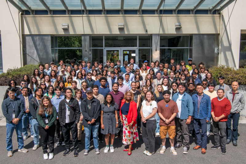
As part of a long-standing tradition of nurturing the next generation of particle accelerator scientists and engineers, the Accelerator Technology & Applied Physics (ATAP) Division at the U.S. Department of Energy (DOE)’s Lawrence Berkeley National Laboratory (Berkeley Lab) and the Lab’s Workforce Development & Education (WD&E) Office hosted 120 student interns at Berkeley Lab. Their visit included guided tours of the Lab’s BELLA Center, Advanced Light Source, and other user facilities. In addition to these outreach and education efforts, ATAP hosted 16 WD&E Office interns and participated in a WD&E Office-led poster session held in August.
“The strength of our internship programs lies not only in the cutting-edge research projects our interns undertake but also in the immersive experiences that foster a deeper understanding of team science and collaboration,” says Faith Dukes, director of K-12 STEM Education Programs at the Government & Community Relations Office and WD&E Office laboratory education director.
By incorporating tours of facilities like BELLA and the ALS, adds Dukes, “we can provide a more comprehensive learning experience that complements hands-on research projects. These interactions with Berkeley Lab staff not only demystify the research process but also instill a sense of community and shared purpose, empowering our interns to become effective contributors to the scientific ecosystem.”
The tours, held throughout June and July, included undergraduate and graduate interns from the Community College Internship (CCI), Science Undergraduate Laboratory Internship (SULI), Visiting Faculty Program (VFP), Foundry Undergraduate Summer Experience, and SEED Scholars @ LBNL programs. The DOE Office of Science Workforce Development for Teachers and Scientists program sponsors the CCI, SULI, and VFP programs. These programs allow students to collaborate with Berkeley Lab researchers and technical staff on projects, explore potential career paths at the Lab and across the DOE complex, become part of the professional community in their field, and form new friendships.
“I’m passionate about our internship programs at Berkeley Lab, in part, because I got my start here as an intern in the CCI and SULI programs,” says Laleh Coté, a STEM education program manager at WD&E who helped guide the tours. “Additionally, programs like these can change someone’s life by immersing them in a new professional environment and deepening their understanding of how people collaborate on large-scale scientific endeavors.”
During the 10-week summer internships, Coté notes that the interns—who work in both operations and scientific divisions at the Lab—gain valuable insights into the Lab’s extensive research capabilities and the community of experts. “Many of our interns are undergraduates, and it’s valuable for them to explore different career pathways they could pursue after their studies. The tours are a key part of this discovery process.”
A key part of these internships involves touring the cutting-edge facilities at the Lab and learning from our world-renowned experts. These include the BELLA Center, a global hub of excellence in laser technologies and their applications, such as next-generation particle accelerators based on laser-plasma acceleration. It also houses ATAP’s state-of-the-art BELLA Petawatt (PW) laser, which can deliver 40 Joule pulses lasting tens of femtoseconds (millionths of a billionth of a second).
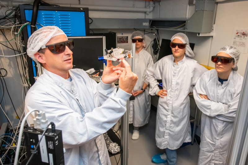
“The students were very receptive, asking questions the whole time,” says Jeroen van Tilborg, a BELLA senior scientist and deputy director for experiments, who led the students during the July 2 guided tour of the BELLA PW laser bay and accelerator cave. “They understood the concept of making accelerators more compact and affordable, and these advanced laser-plasma accelerators (LPAs) could enable new and exciting applications.”
He continues, “It’s good to see the next generation excited about accelerator science and applications. If anything, I hope they bring a passion for high-power lasers and novel accelerator techniques to the next steps in their career. They could be the next LPA scientist or the next user of LPA radiation sources.”
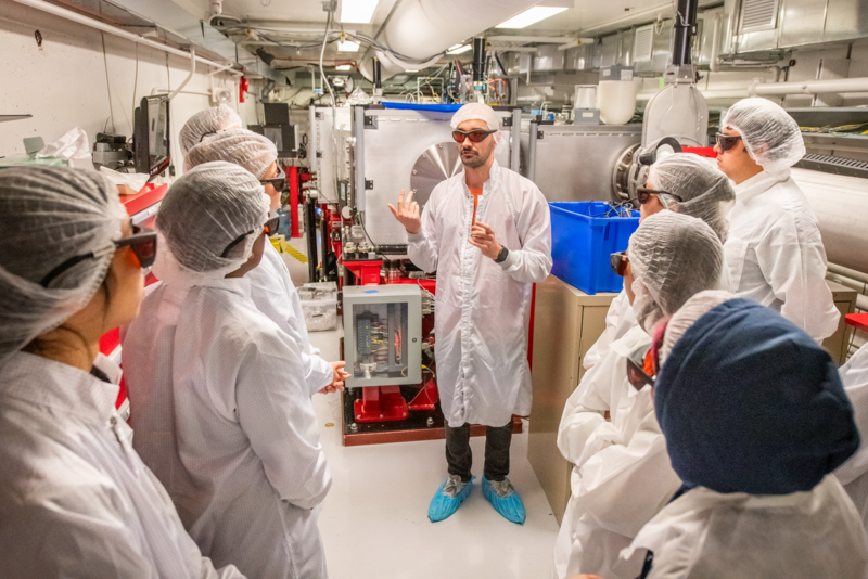
During their second tour of BELLA, on July 10, BELLA Research Scientist Aodhan McIlvenny explained how the center’s high-power lasers differ from those in everyday use and how these lasers are used to drive advanced laser-plasma accelerators (LPAs).
“The physical size of these lasers, along with their peak laser power, attracted a lot of attention from the students,” notes McIlvenny. “After showing the laser, I demonstrated how precise we must be when aligning this large laser beam and focusing it through a pinhole that serves as the entrance to our accelerator, with a laser spot the width of a human hair.”
This demonstration, he adds, showed how changing the focus of the laser and the type of plasma that’s generated can drive multiple types of radiation sources for various applications, proving just how versatile these LPAs can be.
Coté says, “This was an enjoyable experience for the interns and gave them a first-hand look (and some selfies) inside the BELLA Center. I expect that this tour will inspire some of them to apply for internships or jobs with BELLA in the future.”

Student interns tour the Advanced Light Source facilities. (Credit: Brieanna Wright)
The students also visited the Lab’s Advanced Light Source (ALS), a synchrotron light user facility supported by the DOE’s Basic Energy Sciences Program, which has over 40 beamlines serving nearly 1,700 users annually across physical and life sciences.
“The tours for the interns are always a lot of fun,” says ATAP’s Outreach and Communications Specialist, Ina Reichel, who led the tours of the ALS. “They are interested in seeing the ALS and learning about the cool science that’s happening here. And they ask great questions beyond the perennial ‘What’s with all the foil?’”
According to Coté, many interns return to the Lab for a second internship within a year, or later on as a graduate researcher, postdoctoral student, or employee. In this way, she says, these internships “are important stepping stones to the next phase of their career,” adding that “those interns who go on to pursue different career pathways will have learned about how DOE national laboratories work, and may collaborate with us indirectly as advocates.”
Dukes says, “Our research and communications colleagues play a vital role in this effort, supporting our goal of preparing the next generation of scientists and engineers for the complexities of modern research and cultivating a culture of collaboration and innovation.”
To better support the Lab’s commitment to developing the next generation of scientists, engineers, and STEM professionals, the Lab is consolidating the K-12 STEM Education & Outreach programs and the WD&E Office within the Lab Directorate. Dukes will serve as the office’s director.
These changes, says Dukes, will be implemented in phases, with the new office becoming fully operational in the fall. This new consolidated structure will enhance efficiency and offer a more consistent experience for everyone involved; it will coordinate how the Lab supports interns across the organization and also strengthen relationships with teachers, faculty, and those in technical and operations roles.
The organizers would like to thank the other staff members who participated in the tour, including Asmita Patel, ATAP deputy division director for operations, who organized these outreach and education efforts for ATAP and welcomed students at the WD&E orientation on June 2.
For more information on ATAP News articles, contact caw@lbl.gov.