
Modern particle accelerators provide unprecedented control and precision for exploring matter at the atomic level. This capability enables researchers to deepen our understanding of the fundamental interactions between radiation and materials, supporting advancements across various fields. These advancements include the development of radiation-tolerant materials, detectors, and electronics for applications in quantum information science (QIS)—an emerging field that promises to transform computing, communications, and security and usher in a new era of scientific innovation and discovery. Additionally, this research could have potential applications in high-radiation environments, such as future fusion reactors.
Now, researchers from the Accelerator Technology & Applied Physics (ATAP) Division at the Department of Energy’s Lawrence Berkeley National Laboratory (Berkeley Lab) and colleagues from the Centro Nacional de Aceleradores and the departments of Atomic, Molecular, and Nuclear Physics and Applied Physics II at the University of Seville, in Spain, are using intense, ultrashort pulsed ion beams from particle accelerators to explore the formation and recombination of defects in silicon diodes.
The work offers new insights into the dynamics of defect formation in semiconductors and could further the development of optical qubits for applications in QIS. It has been featured in a chapter titled “Dynamics of Radiation Effects in Silicon Studied with Pulsed Ion Beams and Ion Beam Induced Charge Collection” in a new book, Applications of Accelerators in the Quantum Technology Era (CRC Press, November 2024). The book, released on November 12, 2024, resulted from a project coordinated by the International Atomic Energy Agency and highlights the latest research on radiation-induced effects and ion-solid interaction processes for designing novel quantum materials for future quantum technologies, such as quantum information processors and integrated quantum repeaters.
“When ions from intense, short pulses interact with a semiconductor like silicon, they can transfer energy to the atomic structure,” explains Thomas Schenkel, a senior scientist in ATAP’s Fusion Science & Ion Beam Technology (FS&IBT) Program and a co-author of the chapter. “This energy transfer disrupts the arrangement of atoms, leading to defects, interstitials, and vacancies in the crystal lattice.”

The target chamber for irradiating silicon diodes with intense, ultrashort pulses ion beams at Berkeley Lab. (Credit: Berkeley Lab)
While defects in silicon can negatively impact its electronic properties, potentially diminishing the performance of devices like radiation detectors, solar cells, and integrated circuits, Schenkel notes that “not all defects created by nonionizing energy loss are harmful; some can lead to desirable properties, such as light emission.”
Light-emitting defects, called quantum emitters or color centers, can be stable and efficient single-photon sources. These color centers can couple photons and the spin states of electrons and nuclei, making them promising candidates for developing optical qubits for quantum applications. For example, they can be used in quantum networking, which enables the transmission of quantum information over long distances with minimal loss.
Furthermore, integrating established silicon manufacturing techniques from the electronics industry with the properties of color centers could create new opportunities for fabricating hybrid classical-quantum devices that utilize the strengths of both domains.
Schenkel says this synergy “could potentially drive innovation in semiconductor technology and QIS, accelerating the development of practical quantum technologies and facilitating their widespread adoption.”
Pulsed ion beams and defect engineering
Recent advancements in ion particle acceleration techniques have enabled new capabilities for generating intense, short-lived ion pulses. These pulses can exceed one hundred billion (1011) ions per pulse per MeV, with durations ranging from picoseconds to nanoseconds. This progress has transformed the study of radiation-induced effects on materials and enhanced techniques such as defect engineering—the intentional introduction of structural defects into materials—particularly for applications in QIS and for studies of radiation resilience in electronic devices.
Although significant progress has been made in quantifying the formation of radiation-induced defects in silicon devices, accurately predicting the extent of structural damage and defect formation “is still a major challenge,” says Arun Persaud, a senior scientist and head of FS&IBT, who is a leading experimentalist in the research and a co-author of the chapter.
“This,” he explains, “is a result of the complex interactions between the incoming radiation and the silicon lattice, which influence the formation of color centers in silicon. Several factors contribute to this process, including the type of ion, its energy, the flux of the ion beam, the temperature of the silicon, and the type and concentration of impurities present in the lattice. Additionally, pre-existing defects can either promote or inhibit the formation of secondary defects, affecting the overall extent of color center formation.”
While conventional ion implanters generally operate with continuous ion beams at fluxes significantly below 10¹⁶ ions per square centimeter per second (cm⁻² s⁻¹) to introduce dopant atoms into the silicon lattice or to create defects, the researchers employed pulsed beams of 1 MeV helium (He⁺) ions with fluxes varying by 11 orders of magnitude. Using pulsed beams enabled them to irradiate the diodes with dose rates as high as 10¹⁹ ions cm⁻² s⁻¹.
To generate these intense, ultra-short bursts of ion beams in precise and targeted doses for delivering high-flux irradiations, the researchers utilized Berkeley Lab’s Neutralized Drift Compression Experiment (NDCX-II) linear accelerator. Additionally, they employed ATAP’s BELLA Center laser-plasma acceleration facilities to create powerful short-pulsed ion beams, expanding the parameter domain to encompass more ion species and a broader range of ion energies.
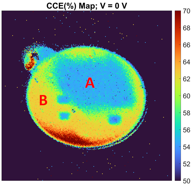
Mean CCE map of the diode after sequential low and high ion flux irradiation. This shows a hot spot (the blue region marked as “A”), while the rest of the diode was irradiated with a lower fluence (yellow zone marked as “B”).
Low He+ ion flux control irradiation and ion beam-induced charge (IBIC) measurements were conducted using 108 ions cm⁻² s⁻¹ dose rates. These experiments utilized the 3 MV Tandem accelerator at the Centro Nacional de Aceleradores, employing a nuclear microprobe in experiments led by Javier Garcia Lopez. A professor of nuclear physics at the University of Seville and scientific coordinator for the Centro Nacional de Aceleradores, he is also the lead author of the chapter.
After irradiating the diodes with pulsed ion beams, the researchers used the IBIC technique to measure the resulting charge collection efficiency (CCE) in the silicon devices. This allowed them to compare the changes in the diodes’ CCE and to quantify variations in defect accumulation caused by irradiations with different ion fluxes or dose rates.
Schenkel says, “These capabilities are crucial for evaluating the resilience and performance of semiconductor devices under extreme conditions, facilitating the development of more robust and reliable electronic components for use in space exploration, nuclear reactors, and other challenging environments.”

CCE for PIN diodes irradiated with high (single pulse) and low ion flux.
By analyzing the movement of charge carriers, such as electrons and holes, through the damaged regions, “we gained detailed insights into the formation and behavior of defects,” says Persaud. “Our analysis showed that the likelihood of electron trapping increased threefold when exposed to high-flux ion pulses compared to conventional low-flux irradiations.”
Additionally, they discovered that defect accumulation intensified at ion fluxes of approximately 2 x 10¹⁹ ions cm⁻² s⁻¹. Furthermore, high-flux ion pulses were found to partially anneal pre-damaged samples by inducing intense local excitations and heating.
According to Schenkel, combining intense, short ion pulses from NDCX-II or laser-plasma acceleration with IBIC and other testing techniques “presents exciting new opportunities in defect engineering and is significant for applications in quantum technologies, as qubits can be formed from defects that necessitate precise control over their atomic structure.”
He adds that the work provides a deeper understanding and greater control over the spatial and temporal dynamics of defect formation and recombination in semiconductors. “This could lead to the discovery of new quantum emitters that exhibit enhanced stability and coherence of quantum states, thereby laying the groundwork for more reliable and scalable technologies in quantum computing, communication, and sensing.”
The chapter’s other co-authors included Qing Ji (ATAP), Carmen Jimenez Ramos (Centro Nacional de Aceleradores and the Department of Applied Physics II at the University of Seville), and Adrian Garcia Osuna and Mauricio Rodriguez Ramos (Centro Nacional de Aceleradores).
The Department of Energy, Office of Fusion Energy Science, funded the research presented here. The International Atomic Energy Agency supported the collaboration between Berkeley Lab and the University of Sevilla as part of the Coordinated Research Project “Ion Beam Induced Spatio-temporal Structural Evolution of Materials.”
To learn more …
New Technique Could Help Build Quantum Computers of the Future
Advances in Quantum Emitters Mark Progress Toward a Quantum Internet
Lasers, Ions, and Silicon: Expanding the Toolkit and Building Blocks for Quantum Information Science
For more information on ATAP News articles, contact caw@lbl.gov.