Key Takeaways
- Researchers have shown that high-energy ion beams can form one-dimensional chains of closely spaced color-center qubits in semiconductors.
- The research could lay the groundwork for scalable qubit assemblies for future quantum processors.
- The technique could advance quantum computing, serve as the backbone for a quantum internet, and be used in sensing applications to support progress in fusion.
Quantum technologies could usher in a new era of scientific discovery, driving advancements in computing, communications, sensing, and many other fields. Quantum computers, for example, could perform complex calculations far beyond the capabilities of even today’s most powerful supercomputers, leading to breakthroughs from medicine to science. Quantum sensors could offer unprecedented levels of precision, significantly improving navigation and medical imaging. A quantum internet promises increased speeds and enhanced security.
While the idea of a quantum revolution is exciting, creating reliable, robust, and scalable quantum bits (qubits)—the fundamental building blocks of quantum technologies—remains a significant challenge. Furthermore, to unlock the full potential of quantum computing, these qubits must be coupled together in their thousands or even millions, making the task even more formidable.
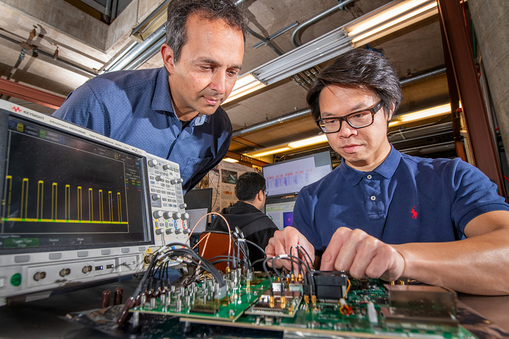
Now, an international team of researchers led by scientists from the Accelerator Technology & Applied Physics (ATAP) Division at the Department of Energy’s Lawrence Berkeley National Laboratory (Berkeley Lab) has used a beam of high-energy, heavy ions to create chains of closely linked color center qubits in diamond. These color-center qubits have demonstrated the potential to form chains of thousands of coupled qubits, opening the door to future quantum computing and quantum sensing applications.
One of the key challenges for realizing quantum computing “is creating assemblies of many qubits in which the qubits couple efficiently with each other,” says Wei Liu, a project scientist in ATAP’s Berkeley Accelerator Controls and Instrumentation Program, who led the research. By successfully coupling large numbers of qubits, quantum scientists hope to unlock the potential of quantum computing.
While many types of qubits are being developed, from superconducting to trapped-ion qubits, Liu says that color center qubits embedded in semiconductors are “one of the leading candidates to create scalable, fault-tolerant qubits to make quantum devices, such as quantum registers and quantum processors, for future quantum computers.”
The research, reported in the journal Communications Materials, is a collaboration among ATAP, Berkeley Lab’s Earth and Environmental Sciences Area, and the Berkeley Lab Molecular Foundry, the University of Helsinki in Finland, the Helmholtz Centre for Heavy Ion Research, the Technical University of Darmstadt, and Leipzig University in Germany.
“This exciting new research illustrates how Berkeley Lab scientists and engineers, working with international partners, harness the capabilities of particle accelerators to advance quantum technologies that promise progress in energy, medicine, science, and other areas,” says ATAP Division Director Cameron.
Strings of “self-aligned” color centers
Color centers are tiny defects introduced into the crystal structure of a material such as diamond. The defect of particular interest for making qubits is a nitrogen atom next to a vacancy in the diamond lattice. When a passing ion transfers energy to the diamond lattice, so-called nitrogen-vacancy (NV) centers can form.
While the traditional method for creating NV-centers involves using relatively low-energy ions, these ions scatter when they enter the diamond, and so “will not produce the directional ion trajectories along which a string of vacancies can form self-aligned NV-centers,” explains Liu.
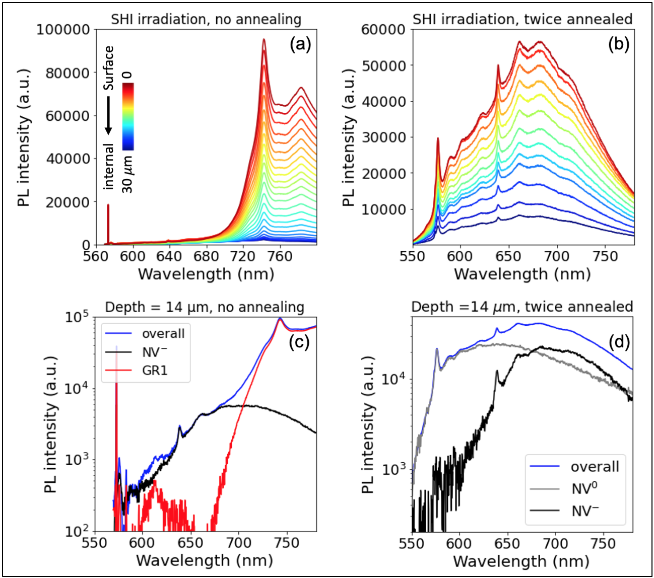
To create NV-centers in diamond, the researchers used the Universal Linear Accelerator at the Helmholtz Centre for Heavy Ion Research in Darmstadt, Germany, to direct 1-GeV gold and uranium ion beams onto a single-crystal nitrogen-doped diamond.
As these high-energy, heavy ions—known as swift heavy ions (SHI)—move through the diamond, the ion beams excite and ionize electrons in the lattice structure through a process called electronic stopping, which transfers energy to the lattice atoms. This rapid energy transfer causes atomic displacements, leading to vacancies formed along the SHI track.
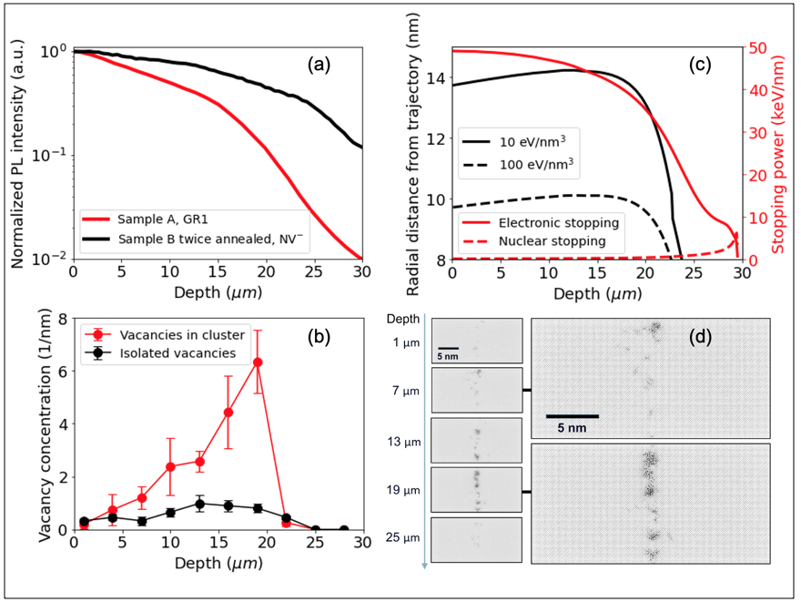
At room temperature, vacancies are relatively immobile, so they remain as isolated defects. However, heating the diamond to about 1000° C—a process called thermal annealing—causes vacancies to diffuse through the lattice, where they encounter substitutional nitrogen atoms, which are fixed in place during diamond growth.
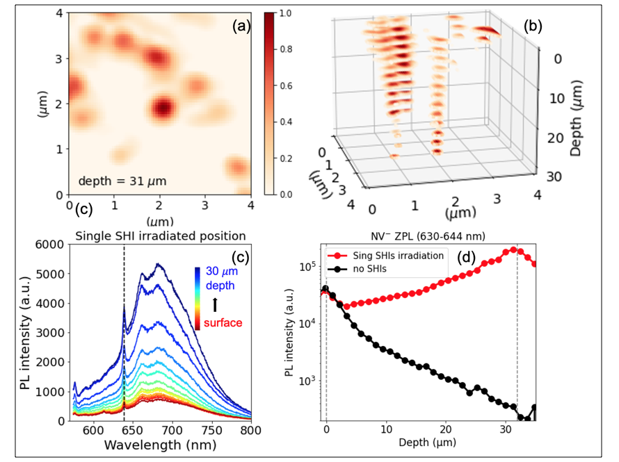
When these vacancies reach nitrogen sites, they bond to the nitrogen, and a chain of NV-centers, a few tens of microns long, forms. Using a diamond wafer with a nitrogen density of about 200 parts per million, the nitrogen atoms are much closer together, allowing dense NV-centers only a few nanometers apart to form along the ion trajectories.
This nanometer spacing between the NV-centers, says Liu, is necessary “to achieve entanglement of the electron spins from neighboring centers: that’s why we need to have a high density of NV-centers.” Without this entanglement, he adds, quantum information “cannot be encoded and transmitted along the chain for quantum computing.”
Creating optical qubits
NV-centers can also emit photons that are inherently entangled with the electron’s spin to create optical qubits.
To create optical qubits, the team initially used a continuous wave laser to excite the NV-center’s electron spin from the ground state to a higher-energy state. This process “resets” the NV-center to a specific initial spin state, similar to setting a switch to a known position before use.
The NV-center’s response to the laser depends on its spin state, with one state emitting bright light and another producing little or no light. A microwave pulse is then used to change the spin state, effectively flipping the quantum switch. Another laser pulse then excites the “bright” spin state, which then emits photons. This laser–microwave combination converts NV centers into optical qubits.
The emitted photons can be “collected and used as carriers of quantum information,” says Liu, enabling spin–photon devices for quantum communication, photonic-based quantum computing, and quantum sensing applications. Furthermore, he adds that these photons “can be transmitted through existing optical fiber networks to carry quantum information,” which could serve as the backbone of a quantum internet.
Additionally, because NV-centers in diamond are highly durable, they retain their quantum sensing capabilities even under extreme radiation and temperature conditions. Therefore, arrays of NV-centers could be embedded into fusion reactor components “to perform real-time, high-resolution magnetic field and temperature mapping,” says Liu, aiding in monitoring plasma behavior and detecting instabilities.
“Color centers in diamond have become a workhorse for early applications of quantum sensing, and they are promising candidates for large-scale qubit integration,” says Thomas Schenkel, a senior scientist in ATAP and principal investigator for the research. “The discovery of NV-center formation in self-aligned chains along the tracks of high-energy, heavy ions inspires new qubit architectures with thousands of coupled NV-centers.”
The team plans to use magnetic fields to control the couplings between NV-centers along the chains, “so we can turn these couplings on and off like a switch,” he says. “We also aim to explore how these chains of color center qubits transmit quantum information, and how localized quantum states might be useful for developing quantum registers and memories.”
The research presented here was primarily supported by funding from the U.S. Department of Energy’s Office of Science, Office of Fusion Energy Sciences. Work at the Molecular Foundry was supported by the Office of Science, Office of Basic Energy Sciences. The optically detected magnetic resonance experiments were performed at the geoscience quantum sensing laboratory at Berkeley Lab, supported by the Office of Science, Office of Basic Energy Sciences, Chemical Sciences, Geosciences, and Biosciences Division.
To learn more…
Wei Liu, Aleksi A. M. Leino, Arun Persaud, Qing Ji, Kaushalya Jhuria, Edward S. Barnard, Shaul Aloni, Christina Trautmann, Marilena Tomut, Ralf Wunderlich, Chloé Nozais, Saahit Mogan, Hunter Ocker, Nishanth Anand, Zhao Hao, Flyura Djurabekova, and Thomas Schenkel. “Optical and spin properties of nitrogen vacancy centers in diamond formed along high-energy heavy ion tracks.” Commun Mater 6, 242 (2025). https://doi.org./10.1038/s43246-025-00961-6
For more information on ATAP News articles, contact caw@lbl.gov.